A cutting-edge AI acceleration platform powered by gentle slightly than electrical energy might revolutionize how AI is skilled and deployed.
Utilizing photonic built-in circuits created from superior III-V semiconductors, researchers have developed a system that vastly outperforms conventional silicon GPUs in each power effectivity and velocity. This expertise couldn’t solely decrease power prices but additionally scale AI to new ranges of efficiency, probably remodeling every thing from information facilities to future good programs.
The AI Increase and Its Infrastructure Challenges
Synthetic intelligence (AI) is quickly remodeling a variety of industries. Powered by deep studying and huge datasets, AI programs require huge computing energy to coach and function. Immediately, most of this work depends on graphical processing items (GPUs), however their excessive power consumption and restricted scalability pose important challenges. To help future progress in AI, extra environment friendly and sustainable {hardware} options are wanted.
A Leap Ahead: Photonic Circuits for AI
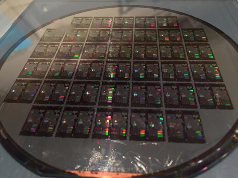
A current examine revealed within the IEEE Journal of Chosen Matters in Quantum Electronics introduces a promising different: an AI acceleration platform constructed on photonic built-in circuits (PICs). These optical chips provide higher scalability and power effectivity than conventional, GPU-based programs. Led by Dr. Bassem Tossoun, Senior Analysis Scientist at Hewlett Packard Labs, the analysis reveals how PICs that incorporate III-V compound semiconductors can run AI workloads quicker and with far much less power.
Not like standard {hardware}, which makes use of digital distributed neural networks (DNNs), this new method makes use of optical neural networks (ONNs), circuits that compute with gentle as an alternative of electrical energy. As a result of they function on the velocity of sunshine and decrease power loss, ONNs maintain nice potential for accelerating AI extra effectively.
“Whereas silicon photonics are straightforward to fabricate, they’re tough to scale for complicated built-in circuits. Our machine platform can be utilized because the constructing blocks for photonic accelerators with far better power effectivity and scalability than the present state-of-the-art,” explains Dr. Tossoun.
The workforce used a heterogeneous integration method to manufacture the {hardware}. This included the usage of silicon photonics together with III-V compound semiconductors that functionally combine lasers and optical amplifiers to cut back optical losses and enhance scalability. III-V semiconductors facilitate the creation of PICs with better density and complexity. PICs using these semiconductors can run all operations required for supporting neural networks, making them prime candidates for next-generation AI accelerator {hardware}.
How the Platform Was Fabricated
The fabrication began with silicon-on-insulator (SOI) wafers which have a 400 nm-thick silicon layer. Lithography and dry etching had been adopted by doping for metallic oxide semiconductor capacitor (MOSCAP) gadgets and avalanche photodiodes (APDs). Subsequent, selective progress of silicon and germanium was carried out to type absorption, cost, and multiplication layers of the APD. III-V compound semiconductors (reminiscent of InP or GaAs) had been then built-in onto the silicon platform utilizing die-to-wafer bonding. A skinny gate oxide layer (Al₂O₃ or HfO₂) was added to enhance machine effectivity, and eventually a thick dielectric layer was deposited for encapsulation and thermal stability.
A New Frontier in AI {Hardware}
“The heterogeneous III/V-on-SOI platform gives all important elements required to develop photonic and optoelectronic computing architectures for AI/ML acceleration. That is significantly related for analog ML photonic accelerators, which use steady analog values for information illustration,” Dr. Tossoun notes.
This distinctive photonic platform can obtain wafer-scale integration of all the numerous gadgets required to construct an optical neural community on one single photonic chip, together with energetic gadgets reminiscent of on-chip lasers and amplifiers, high-speed photodetectors, energy-efficient modulators, and non-volatile part shifters. This allows the event of TONN-based accelerators with a footprint-energy effectivity that’s 2.9 × 10² instances better than different photonic platforms and 1.4 × 10² instances better than essentially the most superior digital electronics.
Remodeling AI with Mild-Pace Effectivity
That is certainly a breakthrough expertise for AI/ML acceleration, lowering power prices, bettering computational effectivity, and enabling future AI-driven purposes in numerous fields. Going ahead, this expertise will allow datacenters to accommodate extra AI workloads and assist clear up a number of optimization issues.
The platform might be addressing computational and power challenges, paving the best way for sturdy and sustainable AI accelerator {hardware} sooner or later!
Reference: “Giant-Scale Built-in Photonic Gadget Platform for Vitality-Environment friendly AI/ML Accelerators” by Bassem Tossoun, Xian Xiao, Stanley Cheung, Yuan Yuan, Yiwei Peng, Sudharsanan Srinivasan, George Giamougiannis, Zhihong Huang, Prerana Singaraju, Yanir London, Matěj Hejda, Sri Priya Sundararajan, Yingtao Hu, Zheng Gong, Jongseo Baek, Antoine Descos, Morten Kapusta, Fabian Böhm, Thomas Van Vaerenbergh, Marco Fiorentino, Geza Kurczveil, Di Liang and Raymond G. Beausoleil, 9 January 2025, IEEE Journal of Chosen Matters in Quantum Electronics.
DOI: 10.1109/JSTQE.2025.3527904